- 您现在的位置:买卖IC网 > Sheet目录336 > LCMXO2280C-C-EVN (Lattice Semiconductor Corporation)BOARD CONTROL EVAL MACHXO
DC and Switching Characteristics
MachXO Family Data Sheet
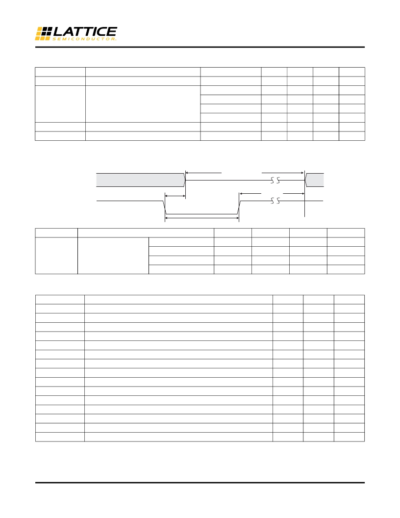
MachXO “C” Sleep Mode Timing
Symbol
t PWRDN
t PWRUP
t WSLEEPN
t WAWAKE
Parameter
SLEEPN Low to Power Down
SLEEPN High to Power Up
SLEEPN Pulse Width
SLEEPN Pulse Rejection
Device
All
LCMXO256
LCMXO640
LCMXO1200
LCMXO2280
All
All
Min.
—
—
—
—
—
400
—
Typ.
—
—
—
—
—
—
—
Max
400
400
600
800
1000
—
100
Units
ns
μs
μs
μs
μs
ns
ns
Rev. A 0.19
Flash Download Time
Power Down Mode
I/O
t PWRUP
t PWRDN
SLEEPN
t WSLEEPN or t WAWAKE
Symbol
Parameter
LCMXO256
Min.
—
Typ.
—
Max.
0.4
Units
ms
t REFRESH
Minimum V CC or V CCAUX
(later of the two supplies)
to Device I/O Active
LCMXO640
LCMXO1200
LCMXO2280
—
—
—
—
—
—
0.6
0.8
1.0
ms
ms
ms
JTAG Port Timing Specifications
Symbol
f MAX
t BTCP
t BTCPH
t BTCPL
t BTS
t BTH
t BTRF
t BTCO
t BTCODIS
t BTCOEN
t BTCRS
t BTCRH
t BUTCO
t BTUODIS
t BTUPOEN
Parameter
TCK [BSCAN] clock frequency
TCK [BSCAN] clock pulse width
TCK [BSCAN] clock pulse width high
TCK [BSCAN] clock pulse width low
TCK [BSCAN] setup time
TCK [BSCAN] hold time
TCK [BSCAN] rise/fall time
TAP controller falling edge of clock to output valid
TAP controller falling edge of clock to output disabled
TAP controller falling edge of clock to output enabled
BSCAN test capture register setup time
BSCAN test capture register hold time
BSCAN test update register, falling edge of clock to output valid
BSCAN test update register, falling edge of clock to output disabled
BSCAN test update register, falling edge of clock to output enabled
Min.
—
40
20
20
8
10
50
—
—
—
8
25
—
—
—
Max.
25
—
—
—
—
—
—
10
10
10
—
—
25
25
25
Units
MHz
ns
ns
ns
ns
ns
mV/ns
ns
ns
ns
ns
ns
ns
ns
ns
Rev. A 0.19
3-15
发布紧急采购,3分钟左右您将得到回复。
相关PDF资料
LDB100-024SW
LED POWER SUPPLY 24V 0-4A 100W
LDB150-048SW
LED POWER SUPPLY 24V-48V 3.125A
LDB200-048SW
LED POWER SUPPLY 24V-48V 4.2A
LDB75-048SW
LED POWER SUPPLY 24V-48V 1.56A
LDS8141-002-T2
IC LED DRIVER WHIT BCKLGT 16WQFN
LDS8160-002-T2
IC LED DVR WHT/RGB BCKLGT 16WQFN
LDS8620-002-T2
IC LED DRIVER FLASH 16WQFN
LDS8621002-T2-960
IC LED DRIVER FLASH 16WQFN
相关代理商/技术参数
LCMXO2280C-L-EV
功能描述:可编程逻辑 IC 开发工具 MachXO 2280C Eval Br d - Standard RoHS:否 制造商:Altera Corporation 产品:Development Kits 类型:FPGA 工具用于评估:5CEFA7F3 接口类型: 工作电源电压:
LCMXO2280C-M-EVN
功能描述:可编程逻辑 IC 开发工具 MachXO Mini Dev Kit RoHS:否 制造商:Altera Corporation 产品:Development Kits 类型:FPGA 工具用于评估:5CEFA7F3 接口类型: 工作电源电压:
LCMXO2280E-3B256C
功能描述:CPLD - 复杂可编程逻辑器件 2280 LUTs 211 I/O 1.2V -3 SPD
RoHS:否 制造商:Lattice 系列: 存储类型:EEPROM 大电池数量:128 最大工作频率:333 MHz 延迟时间:2.7 ns 可编程输入/输出端数量:64 工作电源电压:3.3 V 最大工作温度:+ 90 C 最小工作温度:0 C 封装 / 箱体:TQFP-100
LCMXO2280E-3B256I
功能描述:CPLD - 复杂可编程逻辑器件 2280 LUTs 211 I/O 1.2V -3 SPD
RoHS:否 制造商:Lattice 系列: 存储类型:EEPROM 大电池数量:128 最大工作频率:333 MHz 延迟时间:2.7 ns 可编程输入/输出端数量:64 工作电源电压:3.3 V 最大工作温度:+ 90 C 最小工作温度:0 C 封装 / 箱体:TQFP-100
LCMXO2280E-3BN256C
功能描述:CPLD - 复杂可编程逻辑器件 2280 LUTs 211 I/O 1.2V -3 SPD
RoHS:否 制造商:Lattice 系列: 存储类型:EEPROM 大电池数量:128 最大工作频率:333 MHz 延迟时间:2.7 ns 可编程输入/输出端数量:64 工作电源电压:3.3 V 最大工作温度:+ 90 C 最小工作温度:0 C 封装 / 箱体:TQFP-100
LCMXO2280E-3BN256I
功能描述:CPLD - 复杂可编程逻辑器件 2280 LUTs 211 I/O 1.2V -3 SPD
RoHS:否 制造商:Lattice 系列: 存储类型:EEPROM 大电池数量:128 最大工作频率:333 MHz 延迟时间:2.7 ns 可编程输入/输出端数量:64 工作电源电压:3.3 V 最大工作温度:+ 90 C 最小工作温度:0 C 封装 / 箱体:TQFP-100
LCMXO2280E-3FT256C
功能描述:CPLD - 复杂可编程逻辑器件 2280 LUTs 211 IO 1.2 V -3 Spd
RoHS:否 制造商:Lattice 系列: 存储类型:EEPROM 大电池数量:128 最大工作频率:333 MHz 延迟时间:2.7 ns 可编程输入/输出端数量:64 工作电源电压:3.3 V 最大工作温度:+ 90 C 最小工作温度:0 C 封装 / 箱体:TQFP-100
LCMXO2280E-3FT256I
功能描述:CPLD - 复杂可编程逻辑器件 2280 LUTs 211 IO 1.2 V -3 Spd I
RoHS:否 制造商:Lattice 系列: 存储类型:EEPROM 大电池数量:128 最大工作频率:333 MHz 延迟时间:2.7 ns 可编程输入/输出端数量:64 工作电源电压:3.3 V 最大工作温度:+ 90 C 最小工作温度:0 C 封装 / 箱体:TQFP-100